PANEL-LEVEL PACKAGING EQUIPMENT
Precision at
panel scale.
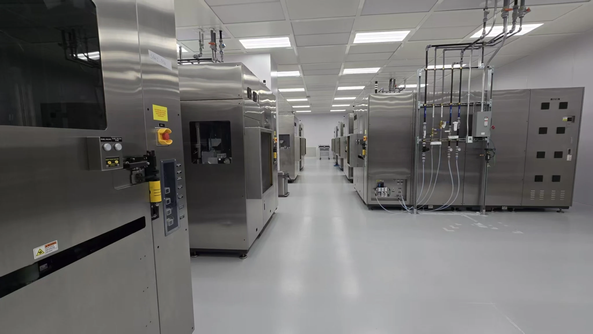
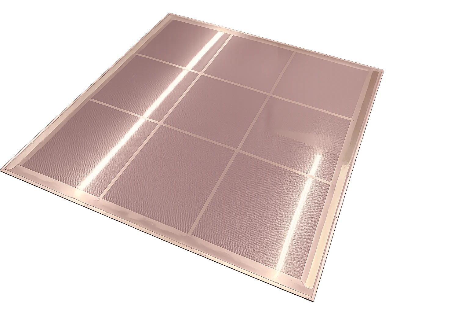
Equipment for panel-level semiconductor packaging: die placement, panel reconstruction, copper taping, compression molding, grinding, die mapping and carrier release or transfer.
the production floor.↘
01 / PANEL PACKAGING TOOLS
Eight tools.
A wider panel perspective.
Explore eight panel packaging tools, from die placement and reconstruction to copper taping and panel processing. Each profile explains engineering features and reference specifications.
Reference figures depend on device, material, recipe and configuration. Final specifications and acceptance criteria are agreed for each application.
02 / THE ENGINEERING INSIDE
Panel scale.
System precision.
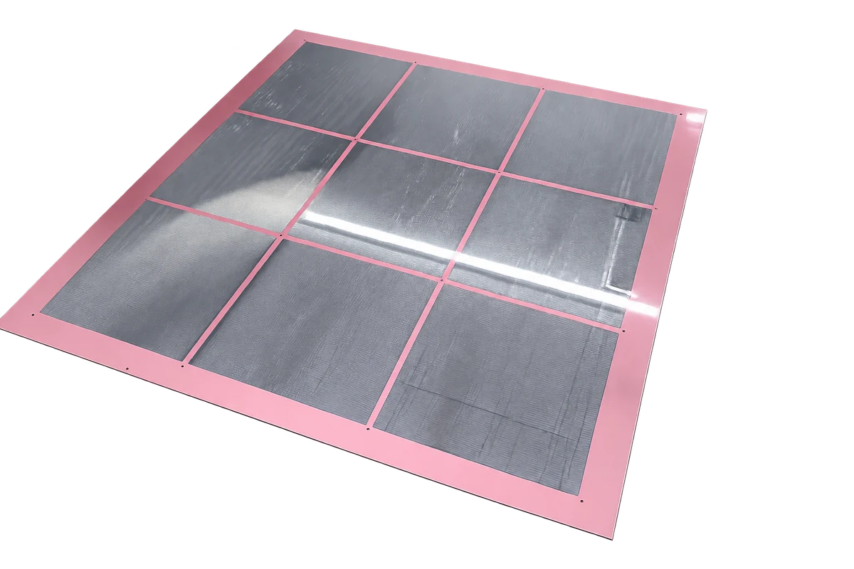
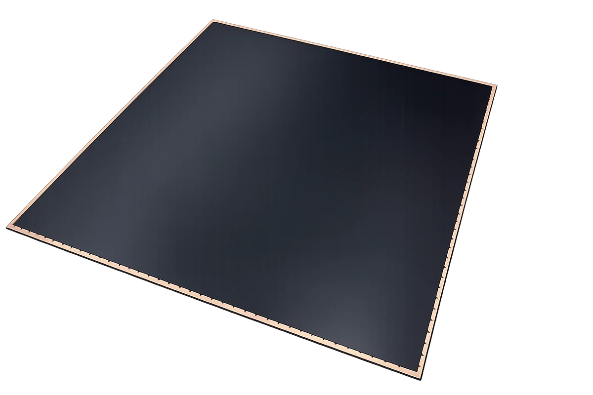
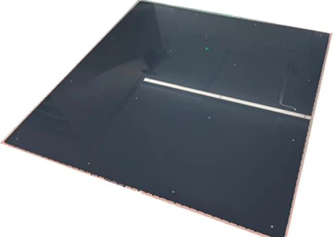
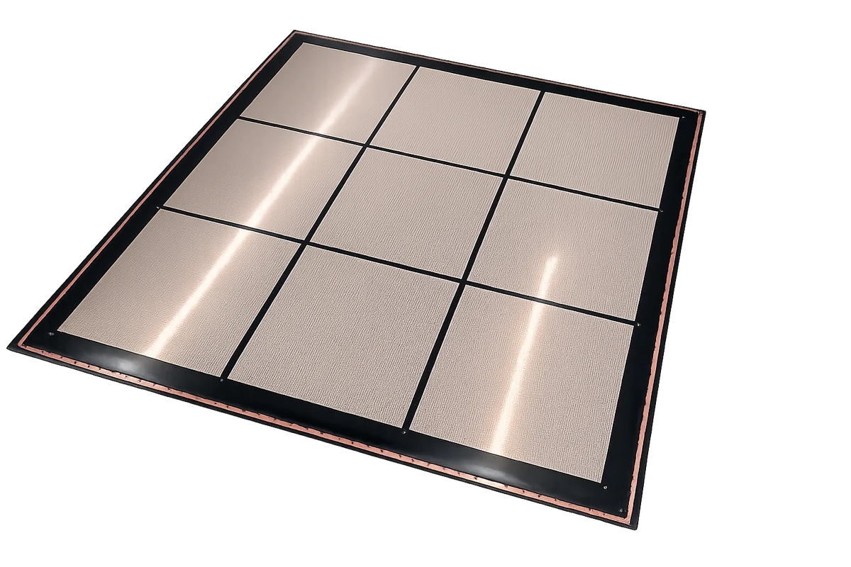
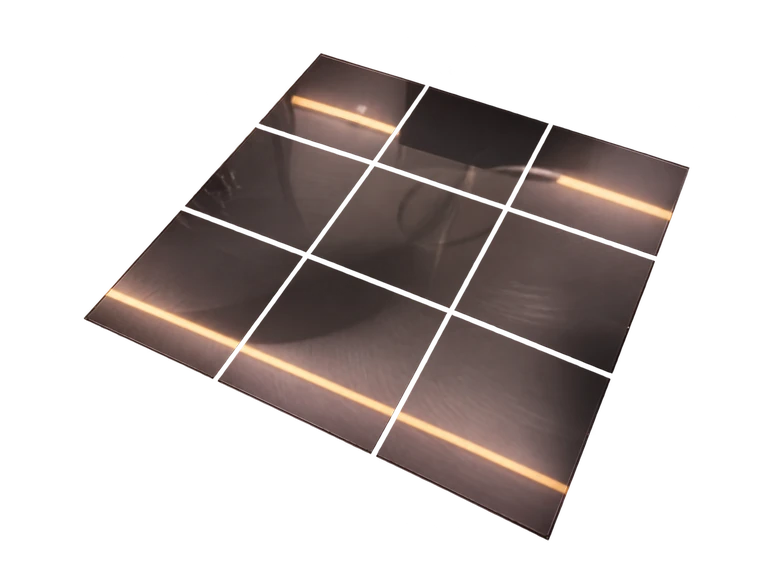
Large panels connect die placement, copper taping, material processing, surface control and carrier handling. We engineer each tool around the workpiece and its next process step.
Placement & metrology
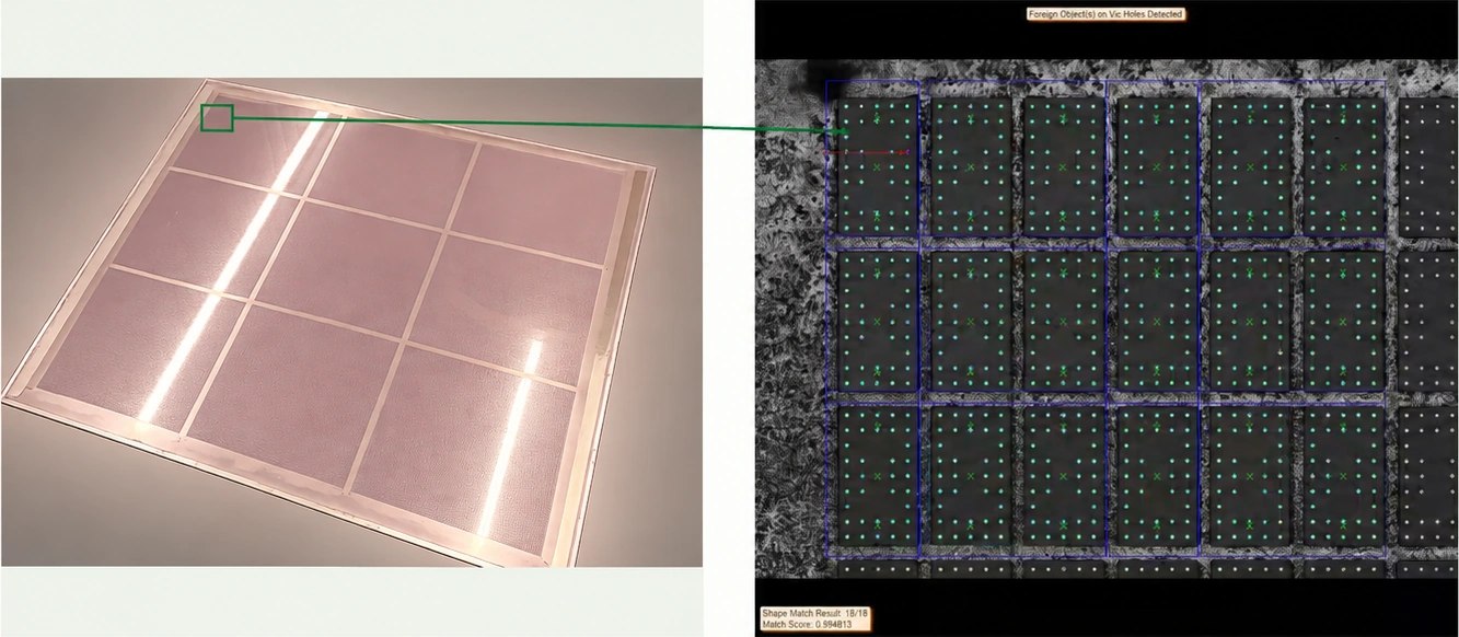
CSX integrates die placement with post-bond inspection and compensation. DLC 700 provides coordinate maps for downstream process alignment.
03 / HOW WE WORK
Your process.
Our shared challenge.
The best equipment starts with a close understanding of the application. We work with your team from the first technical discussion through evaluation and machine integration.
Understand
Define the package, process window and manufacturing requirements together.
Engineer
Translate the application into machine architecture, tooling and controls.
Evaluate
Use sample trials and measurement to review the process and refine the equipment.
Integrate
Align delivery, training and technical support with your implementation plan.
04 / ABOUT PYXIS
Singapore roots.
A wider perspective.
We are a Singapore-based engineering company focused on panel-level semiconductor packaging equipment.
PYXIS combines machine design, motion and vision systems, software and process knowledge. Our panel packaging portfolio spans die placement and reconstruction, copper tape attachment, compression molding, surface finishing, carrier transfer, die-coordinate measurement and release. Engineering and manufacturing capabilities in Singapore and China connect these disciplines around each application.
LET’S BUILD WHAT’S NEXT